Hi-end DC coupled
Circlotron
Hybrid Amplifier
2021
INTRODUCTION
This amplifier born to
try if it is possible increase the sonic performances of the
Amplifier End.
It is the result of many months
of simulations and instrumental testing.
This design is inspired to the
Circlotron
US patent n.
4229706
by James W. Bongiorno and to the
Thorens TEM
3200 by Frank Blöhbaum.
I have used the LTspice free simulation tool to design and optimize this circuit.
The DC servo loop does not follow the Frank Blöhbaum European patent n.
EP1548934B1.
I thank my friend Marco Ferrari Bortolini who designed with me the servo loop
circuit and Michele Branchini who created an incredibly very compact
pcb.
ATTENTION: this is not a project for
beginners because for its stability it must be realized following all
the my layout, it works at very high frequencies.
|
 |
 |
all rights reserved @ copyright -
free only for DIY |
|
 |

The main characteristics
are:
-
dc coupled of all stages
- no capacitors on the signal path
-
high slew-rate about 150V/usec
- high power to drive any
louspeakers, 60W on 8ohm and 120W on 4ohm with the mosfet
ECW20N20
- low distortion with very low feedback
about 10dB
- good damping factor
near to solid state amplifiers, 90mohm with the mosfet
ECW20N20
- large frequency range about 0Hz to 600KHz at -3dB
-
only the input transformer limit the band to 150KHz to eliminate RF
noise
- no switching
output stage like a pure class A, with only 900mA bias current still
17mA with 3A on load
- this is
an amplifier with high efficiency because less than 100W of consumption
per channel
- no matched device are necessary
- only single ended stages
-
only a single output device
-
only a transconductance amplifier with I/V
- only the vaccum tube control the
global feedback
- no high voltage for tubes
only +95V and -155V
- global feedback easy to modify
without high frequency compensation
- full balanced circuit
- it need only an input of 0.5Vrms to get 50W
- the dc servo loop does not change the vacuum tube operating point
-
ultrafast high power discrete Schottky diodes
- regulated power
supply for the driver section
- high transconductance tube,
E180F connected in triode mode
 |
SCHEMATIC
all rights reserved @ copyright - free only for DIY

R
1,R31
10Kohm 3W (min)
R3,R30 5600Kohm 1/4W 1%
R4,R29
1Kohm 1/4W 1%
R9,R25
47ohm 1/2W (on pcb bottom side)
R16,R17
900ohm => 2 x 1800ohm 1/4W 1% in parallel
R10,R23
2350ohm => 2 x 4700ohm 1/4W 1% in parallel
R8,R24
600ohm => 2 x 1200ohm 1/2W 1% in parallel
R11,R21
235ohm => 2 x 470ohm 1/2W 1% in parallel
R6,R27
50ohm => 2 x 100ohm 1/4W 1% in parallel
R2,R32
100ohm 0.5W 1%
R13,R19
100ohm 1/4W 1% for the 2SK1058 or 82ohm for the Exicon 10N20 or 50ohm
for the 20N20
R5,R28
39Kohm SMD 1/4W 1% 1206
R7,R26
10Kohm SMD 1/4W 1% 1206
R15,R18
1000Kohm SMD 1/4W 1% 1206
R12,R14,R20,R22 5Kohm MP925
Caddock
RN1,RN2 1800ohm
1/4W 1%
(on pcb bottom side)
C5,C10
100uF 35V electr. bipolar
C2,C3,C6,C7
1uF SMD Ceramic 50V (Kemet C0805C104M5RACTU)
C1,C12
empty
C4,C11
empty
C8,C9
2.2uF 250V MKP Wima
D1,D2,D3,D4 10V
Zener SMD 3W
T2,T3,T4,T7,T8,T2,T9 MJE15035 PNP
transistor
T5,T6
MJE15034 NPN transistor
IC1,IC2
OPA2277U SMD SOIC
M1,M2
MOSFET 2SK1058 or Exicon 10N20 or
20N20
V1,V2
E180F 6688 Siemens
The parallel of 2 resistors increase the power and the
sonic performances, as alternative use Caddock MK132.
RF1
3400ohm => 2 x 6800ohm 1/4W 1% in parallel
CF1
1000pF silver mica
RG1,RG2
15ohm 3W
CG1,cG2
220pF ceramic
DG1,DG2,DG3,DG4
1N5406
PCB

To add the two
1800ohm
resistors are necessary these modifications on pcb.
photo 6
POWER SUPPLY
The driver stage need a good low ripple regulated power supply
so has been
used is a modification of the original
Michael Maida regulator published on the Texas
Instruments application note.

R19,R26,R20,R22
47ohm 3W
R5,R6
12ohm 3W
R10
27Kohm 2W + 27K 2W
R12
68Kohm 3W
R3,R4
220ohm SMD
1206
R7,R8
137Kohm SMD 1206
R9,R11
1270ohm SMD 1206
R14,R17
953ohm SMD 1206
R15,R18
100ohm SMD 1206
R13,R16
1Kohm trimmer 10 turn
C11,C12,C13,C14 470uF 250V
electr.
C5,C6
10uF SMD
c7,C8,C15,C16,C17,C18 0.1uF 250V MKP
Wima
C3,C4
1uF 250V MKP Wima
C9,C10
2.2uF 250V MKP Wima
C1,C2
empty
B1,B2
KBP408G diode bridge
D3,D4,D11,D12 ,D9,D10 1N40007
Q1,Q2
IRFP240 Mosfet
IC1,IC2
LT3080 SMD SOT-223
KK1,KK2
SK104 heatsink 63.5mm
Here the pcb created by
Michele Branchini.

For the filaments has been used a
LT1083 Postive Adjustable Regulated Power Supply Module
available on
Alixpress shop.

or the better LM317 module with soft-start on
Ebay

For the filaments has been used a LM317 - LM337 Regulated Voltage Power Supply
module available on
Alixpress
shop.

or
this

For the output stage you can use a
simple power supply with only a diode bridge and a capacitor or a CRC or also a CLC
like the
Amplifier End.
There are some choices for the power supply capacitors:
my last choice

Here you can add more capacity using a higher chassie.
I have design a pcb to create a very compact diode bridge
(see also the photos).


INPUT TRANSFORMER
This amplifier need a balanced / differential input created with an input transformers like these.
Taobao
AliExpress
45$ (two pieces)
Alixpress
44$ (two pieces)


From the input transformer to the amplifier module has
been used a CORDIAL CPK 220 Microphone cable, 2 x 0,20 mmq, diam 4,7 mm.

TUBES
It use a pair of good E180F Siemens for each channel,
these are penthode used in triode connecction (g2 connected to anode).
 |
- S = 18mV /V
- Ri = 2.7Kohm
- u = 50
- Vf = 6.3V If =
300mA
- Vg2(max) = 175V
- Ik(max) = 25mA
|
MOSFET
The first mosfet tested in this project is the
2SK1058
Hitachi Renesas, please keep attenction to fake.

The second mosfet tested is the
ECX10N20
Exicon, lower output impedance but also lower dynamic range so to have the
same output power of 2SK1058 you need to increase the power supply voltage of
the output stage.

The last mosfet tested is the
ECW20N20
Exicon, lower output impedance and same dynamic range of the 2SK1058.

CABINET
On paper each lateral heat sink of this chassie have a capacity of 0.25 °C/W so
it will keep the output devices in a good safe area also when the environment
condition are terrible 35 °C.
It is possible use 4 units container but you should use normal power supply
instead of CLC for the output stage because there is no enough space for all the
parts.

In order to dissipate all the heat generated by this
amplifier in my case I chose this container by
HiFi 2000.
Dissipante 04/300B 4U 10mm SILVER
Product
Code: 1NPD04300B
temperature
coefficient 0,31 C°/W per each side

Inner baseplate for Dissipante 300mm
Product Code: 1BASEPD300

I used the HiFi 2000 company for almost all the
mechanical processes and here there are some specifications used for this phase.


If you think to use the last Exicon mosfet enlange the
size 75.7mm to about 80mm otherwise it is necesary bend the pins like this
image.

PROTECTION CIRCUIT
Any serious solid
state amplifier need a protection circuit because a fault on output transistors
or mosfet can destroy the loudspeakers.
This design need also a relay on output terminals to keep disconnected both the
output pins (+ and -)
during the start-up phase at the switch-on for 1min.
I have decided to use 2 x
AIYIMA 2.0 Digital Power Amplifier Speaker Protection Board Delay Relay Speaker
Protection available on Alixpress online shop.
This module use 2
optoisolator
PC817 for each input
and are necessary only some little changes to increase the start-up time, to
increase the accepted input voltage and to obtain a faster reset of timer.


POWER-ON
CIRCUIT

this use the NE555 module from Alixpress

SIMULATIONS


Frequency response simulation with
2SK1058


Follows some models necessary for the simulations.
.MODEL mje15035 pnp IS=5.81508e-15 BF=313.373 NF=0.85
VAF=40.5017 IKF=0.897023 ISE=6.74258e-16 NE=1.04249 BR=0.958017 NR=0.894461
VAR=148.639 IKR=7.05393 ISC=6.74258e-16 NC=2.84461 RB=3.62039 IRB=0.1 RBM=0.1
RE=0.000923293 RC=0.233799 XTB=2.92628 XTI=1.01325 EG=1.17461 CJE=1.5597e-09
VJE=0.99 MJE=0.554057 TF=1.35882e-09 XTF=1000 VTF=467.207 ITF=58.3338
CJC=1.58888e-10 VJC=0.4 MJC=0.23 XCJC=0.786287 FC=0.8 CJS=0 VJS=0.75 MJS=0.5
TR=1e-07 PTF=0 KF=0 AF=1
.MODEL mje15034 npn IS=3.92866e-12 BF=260.938
NF=1.02215 VAF=15.3399 IKF=0.160087 ISE=1e-08 NE=2.54491 BR=26.0938 NR=1.10885
VAR=153.399 IKR=1.60087 ISC=1e-08 NC=1.89024 RB=0.41209 IRB=0.1 RBM=0.41209
RE=0.0001 RC=0.208002 XTB=0.897431 XTI=1.39234 EG=1.206 CJE=1.61534e-09
VJE=0.698417 MJE=0.382854 TF=1.03079e-09 XTF=1000 VTF=100000 ITF=42.9041
CJC=1.04458e-10 VJC=0.441587 MJC=0.23 XCJC=1 FC=0.8 CJS=0 VJS=0.75 MJS=0.5
TR=1e-07 PTF=0 KF=0 AF=1
.MODEL mje350 pnp IS=6.01619e-15 BF=157.387
NF=0.910131 VAF=23.273 IKF=0.0564808 ISE=4.48479e-12 NE=1.58557 BR=0.1
NR=1.03823 VAR=4.14543 IKR=0.0999978 ISC=1.00199e-13 NC=1.98851 RB=0.1
IRB=0.202965 RBM=0.1 RE=0.0710678 RC=0.355339 XTB=1.03638 XTI=3.8424 EG=1.206
CJE=1e-11 VJE=0.75 MJE=0.33 TF=1e-09 XTF=1 VTF=10 ITF=0.01 CJC=1e-11 VJC=0.75
MJC=0.33 XCJC=0.9 FC=0.5 CJS=0 VJS=0.75 MJS=0.5 TR=1e-07 PTF=0 KF=0 AF=1
.SUBCKT 2SK1058 D G S B
M1 D G S B 2SK1058 L=2U W=29.7482M
.MODEL 2SK1058
NMOS (VTO=403.969M KP=20U L=2U W=29.7482M GAMMA=0 PHI=600M LAMBDA=184.988F
RD=60.8251M CBD=2.56138N IS=10F CGSO=1.13517N CGDO=1.13517N TOX=0 NSUB=0 TPG=1
UO=600 RG=50 RDS=1MEG )
.ENDS
.SUBCKT ECX10N20 1 2 3 3
**********************************************
* Model Generated by PEDC *
*Copyright(c) Power Electronics Design Centre*
* All Rights Reserved *
*
Power Electronics Design Centre *
* Dept of Elec & Electronic Engineering *
* University of Wales Swansea *
* Singleton Park *
* Swansea SA2 8PP *
* Tel : +44 (0)1792 295420 *
* Fax : +44 (0)1792 295686 *
* E-mail :
pedc@swansea.ac.uk *
**********************************************
*
Model generated on Dec 6 1999
* MODEL FORMAT: SPICE Level 1
* External
Node Designations
* Node 1 -> Drain
* Node 2 -> Gate
* Node 3 -> Source
*
*
*
M1 9 7 8 8 MM L=1 W=1
* Default values used in MM:
* The
capacitances are added externally
* Other default values are:
* RS=0 RD=0
LD=0 CBD=0 CBS=0 CGBO=0
.MODEL MM NMOS LEVEL=1 IS=1e-32
+VTO=0.473
LAMBDA=0.092 KP=1.585
RS 8 3 0.41
D1 8 9 MD
.MODEL MD D IS=1.0e-32 N=50
BV=250
+CJO=1.0e-9 VJ=0.7 M=0.5
RDS 8 9 1e+06
RD 9 1 0.58
RG 2 7 80
* Gate Source capacitance Cgs0
CAP1 7 8 400e-12
*************************
* Gate Drain capacitance Cdg0
CAP 7 4 10.5e-12
*************************
* Gate Drain Capacitance Cdgj0
* Modelled as a diode
D2 4 9 MDD
.MODEL
MDD D IS=1e-32 N=50
+CJO=94.8e-12 VJ=0.3 M=1
*************************
.ENDS ECX10N20
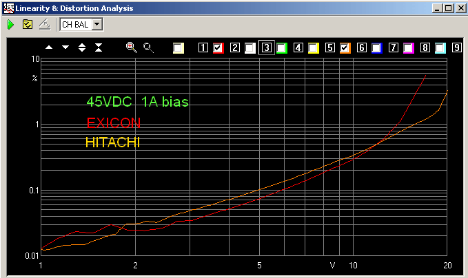
MEASUREMENTS WITH HITACHI 2SK1058 MOSFET
2SK1058 with Rbias = 100ohm and current
about 0.85A thd 0.7% at 21Vrms on 8ohm.
2SK1058 with Rbias = 82ohm and current about 0.6A.
Follow the measurement of distortion decay on 8ohm load,
thd of 0.046% at 3Vrms about 1w.

Follow the measurement of distortion decay on 8ohm load, thd of
0.56% at 21Vrms about 55w.

Follow the measurement of distortion decay on 4ohm load, thd of
1.3% at 17Vrms about 72w.

MEASUREMENTS WITH EXICON 10N20 MOSFET
10N20 with Rbias = 82ohm and current about 0.9A.
The Exicon mosfet
are more easy to find in the marker but these lost more voltage,
here
a test of some years ago.
Follow the measurement of distortion decay on 8ohm load, thd of
0.045% at 3Vrms about 1w.

Follow the measurement of distortion decay on 8ohm load, thd of
0.56% at 16Vrms about 32w.

Follow the measurement of distortion decay on 8ohm load, thd of
1.12% at 18Vrms about 40w.

Follow the measurement of distortion decay on 4ohm load, thd of
2.35% at 12Vrms about 36w.

MEASUREMENTS WITH EXICON ECW20N20 MOSFET
ECW20N20 with Rbias =
50ohm and current about 1.-A.
Follow the measurement of distortion decay on 8ohm load, thd of
0.08% at 5Vrms about 3w.

Follow the measurement of distortion decay on 8ohm load, thd of
0.5% at 23Vrms about 66w.

Follow the measurement of distortion decay on 4ohm load, thd of
2.6% at 22Vrms about 121w.

MEASUREMENT OF FREQUENCY RESPONSE
Follow the measurement of frequency response on 8ohm load,
the
peak on high frequency is generated by the input transformer and it can be
eliminated with a simple RC filter on the secondary.

Here follows the frequency response with 2.2nF after the
grid resistors 1Kohm (not used this filter)

Here follows the frequency response with a RC cell after
the input transformer 3k4ohm (6800//6800) + 1000pF silver mica

This is the real frequency responce of Thorenz TEM 3200
.

FINAL PRODUCT


|
Estimated costs |
| description |
unit price |
quantity |
total (euro) |
| Vacuum tubes E180F |
10 |
4 |
40 |
| 10000uF 35V |
6 |
2 |
12 |
| Components + pcb |
150 |
1 |
150 |
| Input transformers |
22 |
2 |
44 |
| Mosfet |
12.5 |
4 |
50 |
| Chassie with heatsink
and front drilling |
300 |
1 |
300 |
| Vandal Resistant
Push Button |
20 |
1 |
20 |
| Soft-start + termal
protection + relay |
40 |
1 |
40 |
| Power supply modules |
10 |
2 |
20 |
| Transformers |
80 |
3 |
240 |
| Connectors |
25 |
1 |
25 |
| |
|
|
941 |